 Your phone is already way smaller and way more powerful than the first home computers ever were. But progress is progress and IT companies are always looking for a way to make those already tiny chips even smaller and more powerful! Today’s breakthrough by scientists at IBM Research and the California Institute of Technology should help with that…
The two bodies have announced a “scientific advancement” that could be “a major breakthrough” in enabling the semiconductor industry to pack more power and speed into tiny computer chips, while making them more energy efficient and less expensive to manufacture than is currently possible.
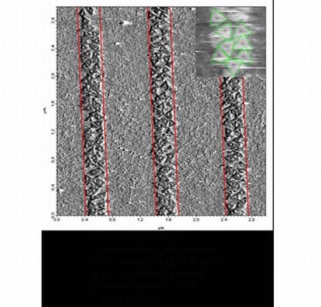
“IBM Researchers and collaborator Paul WK Rothmund, of the California Institute of Technology, have made an advancement in combining lithographic patterning with self assembly – a method to arrange DNA origami structures on surfaces compatible with today’s semiconductor manufacturing equipment,” an official announcement said.
The research was published in a paper called ‘Placement and orientation of DNA nanostructures on lithographically patterned surfaces’, which will be available in the September issue of Nature Nanotechnology or can be found online here.


